

What Does ADTEK’s Optical Interconnect R&D Center Do?
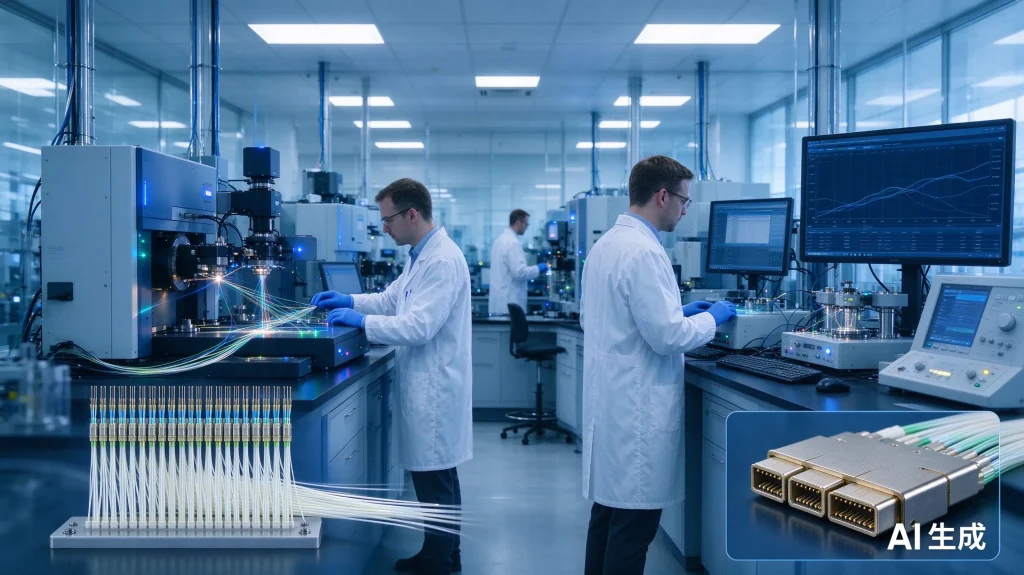
Short answer: ADTEK’s Advanced Optical Interconnect R&D Center accelerates innovation in data center connectivity by providing a dedicated research platform with six specialized laboratories—optical research and testing, precision measurement, reliability validation, sample preparation, assembly and integration, and 3D printing and prototyping—that cover the full product development lifecycle from early-stage research to validation and application deployment. Inaugurated on April 3, 2026, at ADTEK headquarters, the center strengthens the company’s capabilities in data center interconnect solutions and high-performance optical systems.
A Dedicated Platform for Fiber Optic Connectivity R&D
The R&D center was established to support the evolving demands of AI infrastructure and high-speed data transmission. Company leadership emphasized the importance of continuous investment in optical communication solutions and innovation, and the upgraded workspace allows closer coordination between R&D, production, and business units—creating a more integrated development structure for next-generation optical technologies.
At the core of this initiative is a comprehensive research platform designed for end-to-end development of fiber optic connectivity solutions. By improving workspace capacity and fostering a more collaborative environment, ADTEK aims to accelerate innovation and improve efficiency across departments.
Six Laboratories, Full Lifecycle Development
The R&D center includes six specialized laboratories covering optical research and testing, precision measurement, reliability validation, sample preparation, assembly and integration, and 3D printing and prototyping. These facilities support the full lifecycle of product development—from early-stage research to validation and application deployment.
This structure is particularly relevant as optical interconnect technology evolves to serve AI-scale networks. Understanding how optical interconnect is reshaping AI data centers requires exactly this kind of end-to-end testing capability, because new architectures demand validation of both optical performance and mechanical reliability before deployment.
Strengthening High-Speed Optical Interconnect Capabilities
By integrating advanced equipment and cross-disciplinary expertise, the R&D center enables ADTEK to develop high-performance optical products, improve testing and validation processes, accelerate time-to-market, and address challenges in high-speed data transmission. With upgraded infrastructure, ADTEK is strengthening its position in optical interconnect and CPO deployment challenges for AI data centers.
The lab-based approach supports product families that depend on precise optical and mechanical design, including VSFF connectivity solutions for port density, 400G/800G FR4 ROSA assemblies, and 800G optical module packaging. Testing and validation also inform fiber optic polarity methods and connector performance in high-density environments.
Supporting the Future of AI Data Center Infrastructure
As AI-driven data centers continue to scale, the demand for high-speed, reliable connectivity solutions is increasing rapidly. The new R&D center will focus on key innovation areas including high-speed optical connectivity, AI data center infrastructure, and next-generation fiber optic systems.
Architectures such as optical cross-connect (OXC) fundamentals and OXC architecture for AI data center networks benefit from early reliability and integration validation. Likewise, Infinity Flex modules for CPO, OXC, and Roadm depend on precision assembly and measurement capabilities that the center provides.
From Lab to Deployment: How R&D Translates into Reliable Connectivity
For end users, the value of an R&D center is measured by the reliability of deployed products. Precision termination, controlled testing, and validated assembly methods reduce field failures and simplify upgrades. These principles connect directly to guidance such as MPO/MTP connector selection and the packaging, precision termination, and interconnect priorities discussed in ADTEK’s silicon-limit perspective.
The inauguration of the Advanced Optical Interconnect R&D Center represents more than a facility upgrade—it marks the beginning of a new phase in ADTEK’s development. With enhanced resources, improved collaboration, and a clear focus on technology innovation, ADTEK is well positioned to support the next generation of optical communication systems and to deliver reliable, scalable, and high-performance data center connectivity solutions.
These development practices align with the reference frameworks maintained by ITU-T for optical transport networks and TIA for structured cabling, supporting interoperability and long-term deployment confidence.
FAQ
What laboratories are included in ADTEK’s Optical Interconnect R&D Center?
The center includes six specialized laboratories: optical research and testing, precision measurement, reliability validation, sample preparation, assembly and integration, and 3D printing and prototyping.
When was the R&D center inaugurated?
ADTEK officially inaugurated its Advanced Optical Interconnect R&D Center on April 3, 2026, at its headquarters, under the theme “Advancing Together, Opening a New Chapter.”
How does the R&D center support AI data center innovation?
It focuses on high-speed optical connectivity, AI data center infrastructure, and next-generation fiber optic systems, providing end-to-end testing and validation that help bring reliable interconnect solutions to AI-scale networks faster.
Why are reliability validation and precision measurement important for optical interconnects?
Optical interconnects require sub-micron alignment and stable mechanical performance. Reliability validation and precision measurement ensure that products maintain consistent performance under real deployment conditions, reducing field failures and simplifying data center operations.