

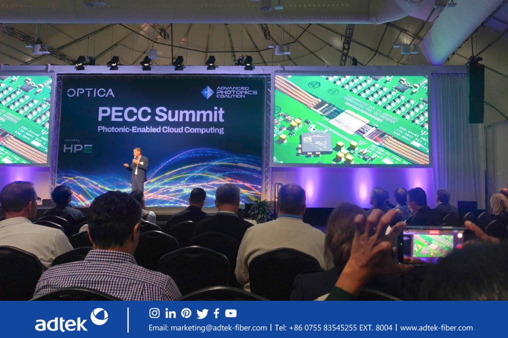
Last week, the Adtek technical and leadership team attended the PECC Summit (Photonic-Enabled Cloud Computing Summit). Co-organized by Optica and the Advanced Photonics Coalition (APC), this closed-door executive and technical gathering brings together leaders across the entire AI compute ecosystem—from hyperscale operators like Google, Microsoft, and Meta to hardware heavyweights like NVIDIA, Arista, Broadcom, and Cisco, alongside leading semiconductor foundries and packaging innovators.
The agenda was focused on a single, pressing imperative: how to scale optical connectivity fast enough to sustain the relentless power and bandwidth demands of multi-gigawatt AI clusters.
For years, the collective assumption in high-speed networking has been that semiconductor physics would do the heavy lifting—pushing lane speeds to 200G and 400G, packing more modulators onto silicon dies, and shrinking laser cavities.
However, across two days of intense technical exchange at PECC, an unmistakable industry consensus emerged: the scaling chokepoint of optical interconnects has officially inverted.
We are no longer held back by optical modulation speed or silicon device physics. With thin-film lithium niobate (TFLN) demonstrating 260+ GBaud reach, multi-wavelength comb lasers slicing single cavities into 16 discrete channels, and 2D micro-VCSEL arrays reaching extreme shoreline densities, optical engines are moving at silicon speed.
The true scaling wall has shifted directly to the physical layer: how do we physically attach, terminate, service, and mass-manufacture hundreds of precision optical fibers at the package boundary at high-volume line rates?
1. The Packaging Paradox and the Mandatory Rise of Detachable FAUs
Co-Packaged Optics (CPO) and Near-Package Optics (NPO) promise transformative efficiency, bringing link energy down from >20 pJ/bit in retimed pluggables to sub-5 pJ/bit. Yet deep physical integration introduces a notorious operational barrier: compounded packaging yield loss.
When an optical engine is permanently attached via fiber pigtails to a multi-tile compute package (such as an XPU or switch ASIC), any assembly defect, micro-crack, or facet contamination on a single fiber strand risks scrapping a multi-thousand-dollar compute module.
Across every major packaging presentation at PECC—from Intel and IBM Bromont to GlobalFoundries and Coherent—the industry verdict was unanimous: optical interfaces at the chip and package boundary must become detachable, field-serviceable, and compatible with multi-point automated testing.
This requirement is appearing across multiple distinct architectures:
- Disaggregated Memory Fabrics: Architecture presentations on Photonic Fabric Memory Appliances (such as Marvell’s PFMA) highlighted 40-fiber (40F) Fiber Array Units (FAUs) linking shared memory pools across 20–30 meters (<300 ns latency) to eliminate KV-cache eviction cliffs in large-scale LLM inference.
- Silicon Photonics Circuit Switches (OCS): Integrated SiPh OCS platforms (scaling from 64×64 chips toward 256-port roadmaps) require thousands of optical breakout fibers at the chassis edge, running into immediate front-panel congestion that legacy MPO geometries cannot resolve.
- Micro-Emitter Engines: Groundbreaking startups developing micro-VCSEL and micro-emitter arrays openly confirmed that while their silicon engines operate flawlessly, the industry lacks standardized receptacles, connectors, and automated cable attachment methods.
The path forward requires moving away from labor-intensive manual assembly toward high-throughput, line-rate passive-alignment termination.
2. The Architectural Fork: “Wide & Slow” vs. “Narrow & Fast”
A standout debate at PECC centered on how physical infrastructure must adapt to severe global supply constraints. Critical substrate materials—most notably Indium Phosphide (InP)—are facing severe shortages, with lead times stretching well into 2027.
Rather than waiting for raw material capacity, the industry is actively hedging across two divergent architectural paths:
- The “Wide & Slow” Paradigm: Spearheaded by the OCP SRMO (Short-Reach Micro-Emitter Optics) track, 1060 nm PCIe-over-optics initiatives, and multi-core multimode fibers (7-core / 19-core MCF). By deploying massive parallel arrays running at lower, power-efficient baud rates, systems eliminate DSP overhead and utilize mature, abundant Gallium Arsenide (GaAs) wafer lines (leveraging established consumer 3D-sensing fabs). However, this creates an explosion in physical fiber counts, demanding ultra-dense 2D array connectors and automated ribbon routing.
- The “Narrow & Fast” WDM Comb Paradigm: Deploying integrated GaAs quantum-dot (QD) comb lasers and external laser modules (ELSFP) to push 8 to 16+ wavelengths into fewer single-mode fibers. This conserves panel beachfront but places extreme precision requirements on thermal wavelength locking and complex optical demuxing.
For interconnect manufacturers, the takeaway is clear: physical infrastructure cannot be single-tracked. Solutions must accommodate both high-fiber-count parallel ribbons and dense single-mode WDM trunks with equal precision.
3. Glass Substrates: The New Frontier of Multi-Die Packaging
Another defining highlight was the cross-industry convergence on glass interposers and glass cores with embedded optical waveguides.
With technology leaders demonstrating ion-exchange waveguides (<0.1 dB/cm loss) across 515×515 mm panel scales, and high-volume advanced packaging lines deploying fan-out interposers with embedded bridge dies, glass is proving to be the optimal substrate to overcome the warpage and thermal expansion limits of organic materials.
Yet, while chip-to-glass coupling is achieving breakthrough results, a crucial commercial void remains unaddressed: How do systems transition light off the edge of a large glass panel into the data center cabling plant?
Developing rugged, high-density, detachable exit connectors at the glass panel boundary represents one of the largest open IP and product opportunities in optical hardware today.
4. Avoiding the Complexity Trap: The Case for Generic Standardization
In an effort to solve sub-micron assembly tolerances, several market approaches have introduced proprietary architectures—such as custom reflective optical bumps etched directly onto customer silicon dies, or serial 3D micro-printing of individual lenses.
While technically sophisticated, proprietary modifications create single-vendor lock-in that hyperscalers consistently resist. Historical precedent shows that cloud builders prioritize multi-source flexibility and standard form factors above all else.
The lasting commercial volume will belong to PIC-agnostic, gang-matable expanded-beam (EBO) interfaces. By utilizing micro-lens arrays that collimate and expand the beam across the connector interface, connections become orders of magnitude more forgiving of dust, lateral misalignment, and thermal vibration:
- Forgiving in the field: absorbing mechanical float and operational debris.
- Precision-engineered in the factory: assembled via automated machine vision, low-outgassing optical adhesives, and deterministic lane-by-lane performance screening.
5. From Cable Chaos to Centralized Optical Shuffles
As AI training and inference clusters expand beyond 100,000 accelerators, manual point-to-point fiber patching inside the rack becomes mathematically and operationally unmanageable.
The industry is rapidly adopting centralized optical shuffles and structured fiber busbars. By embedding complex all-to-all optical routing inside dedicated shuffle chassis and pre-engineered busbar enclosures, operators achieve deterministic failure protection. In an optimized shuffle fabric, an individual trunk failure results in a predictable, graceful degradation (e.g., losing 12.5% of fabric bandwidth) rather than triggering catastrophic, cluster-wide job halts.
The Adtek Perspective: Delivering the Missing Physical Foundation
The discussions at PECC 2026 confirmed our core engineering thesis: the optical computing revolution cannot scale on semiconductor breakthroughs alone; it requires high-volume industrialization at the connector, termination, and packaging layer.
At Adtek, we are directly addressing this transition:
- Accelerating High-Density Shuffle Fabrics: Scaling centralized shuffle boxes and pre-terminated fiber busbar architectures (utilizing MMC, SN-MT, and high-density MT formats) to untangle the scale-up AI backplane.
- Industrializing Passive-Alignment EBO & FAUs: Developing automated, high-throughput termination processes that eliminate labor-intensive active alignment benches and make multi-hundred-channel detachable fiber arrays commercially viable.
- Engaging Open Industry Standards: Actively collaborating within open standardization groups—including the OCP SRMO workstream and the Advanced Photonics Coalition (APC)—to ensure next-generation optical interfaces remain multi-sourced, robust, and manufacturable.
The future of AI computing is optical. We are proud to engineer the physical infrastructure that makes it deployable, scalable, and reliable.