
Reflections from OCP Global Summit 2026: Silicon Bifurcation, the Qualification Squeeze, and the Urgent Race for Interconnect Standards
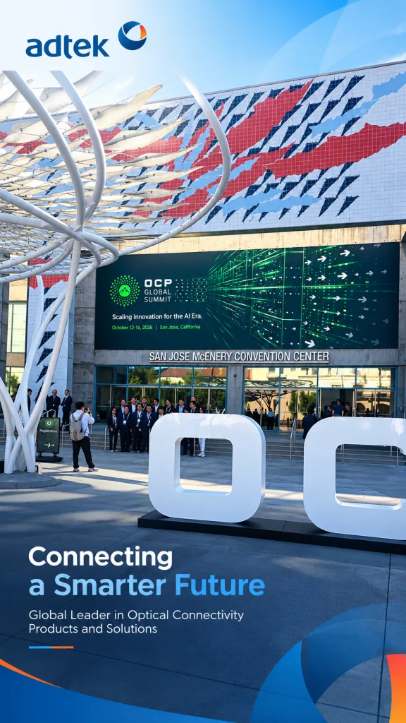
Walking the floor at the 2026 OCP Global Summit in San Jose, one fundamental shift was impossible to ignore: the AI hardware landscape has permanently decentralized.
Where compute once belonged almost exclusively to a dual-vendor stronghold—NVIDIA with GPUs and Google with TPUs—the ecosystem has fractured wide open. Hyperscalers and frontier AI labs are aggressively mitigating single-vendor supply chain and margin risks by bringing custom silicon into production. From OpenAI detailing its custom “Jalapeño” accelerator architecture running over Broadcom Tomahawk 6 fabrics, to Meta’s scaled MTIA deployments, to custom silicon architectures across Microsoft and Alibaba, compute diversity is now the default.
Yet this silicon bifurcation is not occurring in a vacuum. It is colliding head-on with the limits of physical infrastructure, shrinking qualification cycles, and an intense industry-wide push toward open standards.
At ADTEK, tracking and engineering connectivity solutions through this transition requires looking past the marketing slides and examining the raw physical trade-offs. Here is our technical takeaway on where AI interconnects stand today—and where they must go tomorrow.
- The 18-Month Qualification Squeeze vs. Annual Silicon Cycles
A recurring theme across presentations was what systems integrators call “The Squeeze”. Major silicon vendors and hyperscalers now refresh their accelerator architectures roughly every 12 months. However, qualifying a full-scale, multi-rack liquid-cooled AI cluster operating at 224G/lane (and pathfinding toward 448G) takes 18 to 24 months.
When signaling rates climb to 200G+ per lane and cluster power densities push past 1 MW per row, system-level margins evaporate:
- Insertion loss budgetsat the Nyquist frequency leave almost no margin for PCB routing.
- Thermal envelopesat the switch faceplate choke standard air-cooled optics, driving the emergence of direct liquid-cooled pluggables (such as the 12.8T XPO MSA).
- Physical pathway congestionhas reached a breaking point, with intra-datacenter clusters demanding upward of 10 million fiber strands—collapsing standard cable trays and conduit capacities.
With zero room for design iteration loops, proprietary, bespoke hardware architectures have become a massive operational liability.
- The Open Standards Counter-Offensive (MSAs)
The industry’s collective defense against this cycle-time squeeze is an aggressive proliferation of Multi-Source Agreements (MSAs). At OCP 2026, standardization is not merely about consensus; it is the supply chain’s survival mechanism:
- Open CPX MSA:Defining standardized Type 1 and Type 2 sockets for Co-Packaged and Near-Packaged Optics (NPO/CPO), establishing a common mechanical and electrical footprint to decouple the ASIC package from sole-source optical engines.
- 8T XPO MSA:Pushing pluggable form factors into the liquid-cooled era, delivering 4× faceplate density with integrated cold-plate interfaces to protect existing field-serviceable operational models.
- SDM4 MCF MSA:Standardizing 4-core Multi-Core Fiber (MCF) within a conventional 125 µm outer cladding—slashing bulk fiber counts and pathway volume by 4× without altering core geometric handling.
- OCI MSA:Driving consensus on optical compute interconnects to extend the high-bandwidth scale-up domain beyond the single chassis or rack into multi-rack rows.
- Copper and Optics: Co-Design Over Displacement
A common myth in AI networking is that optics will simply eradicate copper. The technical sessions proved the opposite: copper is not dead; it has simply migrated off the motherboard.
At 224G and 448G, transmitting signals through traditional host PCB traces consumes massive loss margins (often 10 dB to 14 dB before reaching a connector). By utilizing direct-to-package copper flyovers (such as near-package cable assemblies and RAF blind-mate backplane interfaces), engineers bypass the host PCB entirely.
This package-launch architecture reclaims up to 18 dB of channel headroom, extending passive copper’s viable reach to 2 to 3.8 meters. As demonstrated in 256-GPU reference fabrics, copper still dominates 100% of internal rack connectivity, while optical engines (whether NPO, CPO, or high-density transceivers) handle the remaining inter-rack scale-up and scale-out traffic. Copper and optics are being co-designed onto the exact same backplane planes.
- The Construction Reality: Fiber Cleanliness, Particulates, and EBO
One of the most candid, pragmatic discussions at OCP 2026 centered on the operational floor: the harsh reality of modern data hall construction.
To meet aggressive go-live deadlines, fiber deployment teams are routinely pulling, dressing, and patching cable assemblies in parallel with mechanical, drywall, and electrical trades. The result is severe airborne contamination: drywall dust, concrete particulate, and ambient debris.
In an AI cluster with millions of optical terminations, contamination is catastrophic:
- A single dust speck on a single-mode core will destroy transmission or permanently damage physical-contact (PC/APC) MT and MMC ferrules under mating spring pressure.
- In synchronous training and low-latency inference workloads, intermittent bit-error degradation (link flapping) forces NCCL collective timeouts, stalling thousands of GPUs and burning tens of thousands of dollars in wasted compute time.
This has triggered a major industry migration toward Expanded Beam Optics (EBO) and contactless lensed interfaces. By expanding the optical beam across a collimating micro-lens array, the optical path becomes virtually dust-resilient, turning what would be a fatal connection block into fractional, harmless attenuation.
However, balancing EBO with tight system-level insertion loss budgets requires careful component engineering. The data center network demands a dual approach: ultra-low-loss physical contact (MT/MMC) for factory-sealed internal shuffles, paired with ruggedized expanded beam technologies where connectors meet the high-risk environments of the faceplate and blind-mate backplane.
How ADTEK is Delivering Value in this Landscape
Navigating this landscape requires more than just analyzing trends; it requires dedicated manufacturing readiness, sub-micron precision, and field-proven reliability.
At ADTEK, our production and engineering roadmap directly targets these exact industry inflection points:
- Ramping 3M™ EBO Production by Q4 2026:To solve the critical data-hall contamination bottleneck, ADTEK is actively ramping volume manufacturing for 3M Expanded Beam Optical (EBO) assemblies by the end of this year. Utilizing 3M’s genderless lensed ferrule design across single-mode and multimode configurations, we are delivering high-density, dust-insensitive optical interconnects that eliminate lengthy field scope-and-clean cycles.
- Active US Conec Engagement on PRIZM® TMT:We are actively engaged in technical training and process validation with US Conec for their cutting-edge PRIZM® TMT lensed ferrule technology. By pairing expanded-beam debris resistance with the ultra-high-density single-mode MMC footprint, this initiative positions ADTEK to deliver next-generation, blind-mate and patch-panel assemblies with an industry-leading optical loss performance.
- Sub-Micron Physical Contact Precision:For internal links where every tenth of a decibel is vital, we continue to tighten interferometric quality controls across our standard MT, MPO, and MMC terminations.
- High-Density Optical Shuffles & Trays:Delivering cleanroom-assembled, custom internal routing cassettes and flex-shuffles that eliminate field mating risks inside dense AI switch and compute chassis.
- Multi-Core Fiber (MCF) Readiness:Developing breakout, fan-out, and termination capabilities aligned with the new SDM4 MCF specifications to help operators de-congest critical intra-datacenter pathways.
The bifurcation of silicon and architectures will continue to accelerate. Success won’t belong to those betting on a single, isolated technology, but to those who engineer flexible, ultra-reliable, standardized interconnect solutions capable of turning raw silicon horsepower into deployed reality.
To discuss your high-density AI interconnect, optical shuffle, or expanded-beam cable assembly requirements, connect with our technical engineering team at ADTEK.
Related articles
Share the page:
Contact US
If you want to know more about us, you can fill out the form to contact us and we will answer your questions at any time.