ADTEK shares | Silicon photonics stocks continue to rise, why is silicon photonics so popular?
Recently, the silicon photonics stock market has been booming, and many investors have flocked in, hoping to get a piece of the pie in this wave of enthusiasm. So, what is the charm of silicon photonics technology that makes the communications field and the investment market so optimistic? Today, let us take a deeper look at silicon photonics technology.

Define
Silicon photonics technology and silicon photonics chips
1. What is Silicon Photonics?
Silicon photonics is a large-scale integrated technology of silicon-based optoelectronics developed using silicon-based materials and using photons and electrons as information carriers. It mainly uses microstructures on silicon wafers to control the transmission and processing of light. The principle of silicon photonics is based on a series of fine circuits and optical components on silicon wafers, including light sources (such as semiconductor lasers), optical amplifiers, waveguides, optical modulators, optical couplers, etc. These components are directly manufactured on silicon wafers through micromachining and lithography technology, and can be assembled into integrated circuit chips and modules.
2. What is Silicon Photonics Chip?
Silicon photonic chips are integrated optical circuits that integrate silicon photonic materials and devices through standard semiconductor processes. They are mainly composed of modulators, detectors, passive waveguide devices, etc. They can integrate multiple optical devices on the same silicon-based substrate, and have the characteristics of high integration, low cost, and high transmission bandwidth. They have unique advantages in terms of size, speed, power consumption, etc. Their processes are compatible with the basic processes of silicon-based microelectronic chips, and can realize optoelectronic 3D integrated chips with silicon-based microelectronics.
Publish
How Silicon Photonics Technology Came into Being
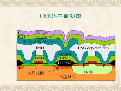
Inspired by integrated circuits, the concept of integrated optical circuits was proposed, which is to use optical waveguides to integrate a series of optoelectronic devices on the same substrate, thereby forming a micro-optical system with certain independent functions. Integrated optical circuits are microelectronic technologies based on silicon CMOS technology. The technology accumulation is very comprehensive, and the silicon-based industry already has strong industrial capabilities. Silicon photonics technology was born by integrating optoelectronic devices using silicon CMOS technology with silicon as the substrate. With the advantages of both microelectronics and optoelectronics, it has become a hot spot for competition among semiconductor and communication companies.

(*Picture from the Internet)
Develop
The development of silicon photonics technology
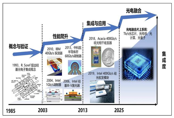
Silicon photonics technology is based on the waveguide theory proposed around 1985. It began to gradually develop from theory to industrialization around 2005-2006. Pioneers such as Luxtera and Kotura have continuously promoted the development of technology and industrial chain, forming a relatively mature fabless industrial chain model of silicon photonics chip foundries (GlobalFoundries, STMicroelectronics, AIM, etc.), laser chip foundries (Uni-Tech, etc.), chip design and packaging (Luxtera, Kotura, etc.). There is also an IDM model represented by Intel, which, except for laser chips, completes the design, silicon-based chip processing, and packaging and testing by itself).

(*Picture from the Internet)
Appliance
Application fields of silicon photonics technology
1. Consumer electronics
In the field of consumer electronics, the high integration characteristics of silicon photonics are very suitable for the needs of consumer electronics, because products such as smart sensors and mobile terminals can use silicon photonics technology to integrate more devices in a limited space, such as smart phones, tablets, etc. Silicon photonics devices have the advantages of high integration and low cost, which can improve the performance and functions of consumer electronic products.

(*Picture from the Internet)
2. High-speed communication
Silicon photonics technology can be used to manufacture high-speed optical modulators and detectors, greatly improving data transmission speeds. It can also realize the multiplexing and demultiplexing of optical signals, further improving the bandwidth and capacity of communication systems. Due to the advantages of silicon photonics such as strong confidentiality, high integration, and suitability for complex optical path control, it can also be applied to cutting-edge fields such as satellite communications and quantum communications, providing strong support for the development of communication technology.
3. Data Center
Data centers require a large amount of data transmission and exchange, and silicon photonics can provide a high-speed, low-energy solution. Optical interconnect devices manufactured using silicon photonics can achieve optical interconnection within and between data centers, greatly improving data transmission efficiency and reducing energy consumption and operation and maintenance costs.
4. Artificial Intelligence and LiDAR
In the field of lidar, silicon photonics technology can produce miniaturized and integrated lidar systems for use in unmanned driving, robotics, intelligent manufacturing and other fields, while greatly reducing the difficulty of verifying solutions.

(*Picture from the Internet)
In addition, silicon-based optoelectronic chips can play the advantages of high bandwidth and low latency in the computational processing of artificial neural networks. When processing a large number of matrix calculation multiplication and addition tasks in deep learning, silicon-based optoelectronic chips have higher processing speeds and lower energy consumption, which is conducive to improving the computational speed and performance of artificial neural networks in deep learning.
5. Biomedicine
Silicon photonic devices have high sensitivity and high precision, which can improve the performance and accuracy of medical equipment. Through the application of silicon photonic technology, highly sensitive biosensors and optical imaging systems can be manufactured for biomolecule detection, cell imaging and disease diagnosis, such as optical imaging instruments, laser treatment equipment, etc.
6. Military Applications
Silicon photonics technology can make data transmission between processor cores 100 times faster or even higher, which can effectively meet the requirements of high-speed military communications for ultra-high transmission rate, ultra-low latency, ultra-high stability, ultra-low cost, and low interference, and can provide high-speed and massive data support for future information-based joint operations. It also shows broad application prospects in the fields of military medicine, military reconnaissance, and military intelligence.
Future
Challenges and prospects of silicon photonics technology
Silicon photonics is a basic supporting technology for emerging industries such as big data, artificial intelligence, and future mobile communications. It is widely used in industries such as big data centers, 5G, and the Internet of Things, and can greatly improve the performance of integrated chips. The future prospects of silicon photonics are very broad, and it will play an increasingly important role in various fields. However, while combining multiple advantages, it also faces some challenges. For example, the optical properties of silicon materials still have certain limitations, and their optical properties need to be further improved.
Looking ahead, with the rapid development of applications such as 5G and data centers, the demand for optical communication technology will continue to grow. The application of silicon photonics technology in optical modules has brought new opportunities for the development of the optical communication field.
With the booming development of silicon photonics, ADTEK , as one of the senior manufacturers in the field of optical communications, is actively committed to promoting the rapid development and widespread application of silicon photonics. With years of professional accumulation, ADTEK will continue to deepen the research and development and innovation of optical communication technology, and continuously bring more abundant and high-quality products to silicon photonics and the entire optical communication field.
We firmly believe that through continuous efforts and innovation, silicon photonics technology will show broader application prospects in the future and contribute more to the prosperity and development of the optical communication industry.
2024.3.15
Recent articles
ADTEK Terminal Box Introduction
ADTEK Terminal Box Introduction The application scenario of the ADTEK Terminal Box (TB) is similar to that of the traditional Access Terminal Box (ATB ),
ADTEK 432F MDC Patch Panel Brief
ADTEK 432F MDC Patch Panel Brief Density:1U 432F Size:44mm(H)x 482mm(W)x 400mm(D) Loaded with 9x 48f MDC module TIA/EIA-568-C.3 RoHS Compliant ISO9001 Certificate Download File Contact
Adtek 40CH 100G DWDM MDC Module
40CH 100G DWDM MDC Module The Adtek Dense Wavelength Division Multiplex Module is designed for DWDM network applications.It is based on the AWG technology and
100G SR4 QSFP28 Optical Transceiver(MDC Interface) Product Specifications
100G SR4 QSFP28 Optical Transceiver(MDC Interface) Product Specifications MDC interface 100G SR4 optical module adopts QSFP package and supports MDC connector cables. 4 groups of
Contact US
If you want to know more about us, you can fill out the form to contact us and we will answer your questions at any time.
